





Category
Exhibition
2026.08.27
Exhibition
BenQ Materials Debuts "Precision Materials for Semiconductor Manufacturing" Platform at SEMICON Taiwan 2026!
Driving High-End Process Yields and Injecting High-Resilience Momentum into Next-Generation Semiconductor Manufacturing.
Leveraging Local Supply Chain and Flexible Customization Advantages to Showcase Customer-Validated and Production-Ready Value with Global Giants.
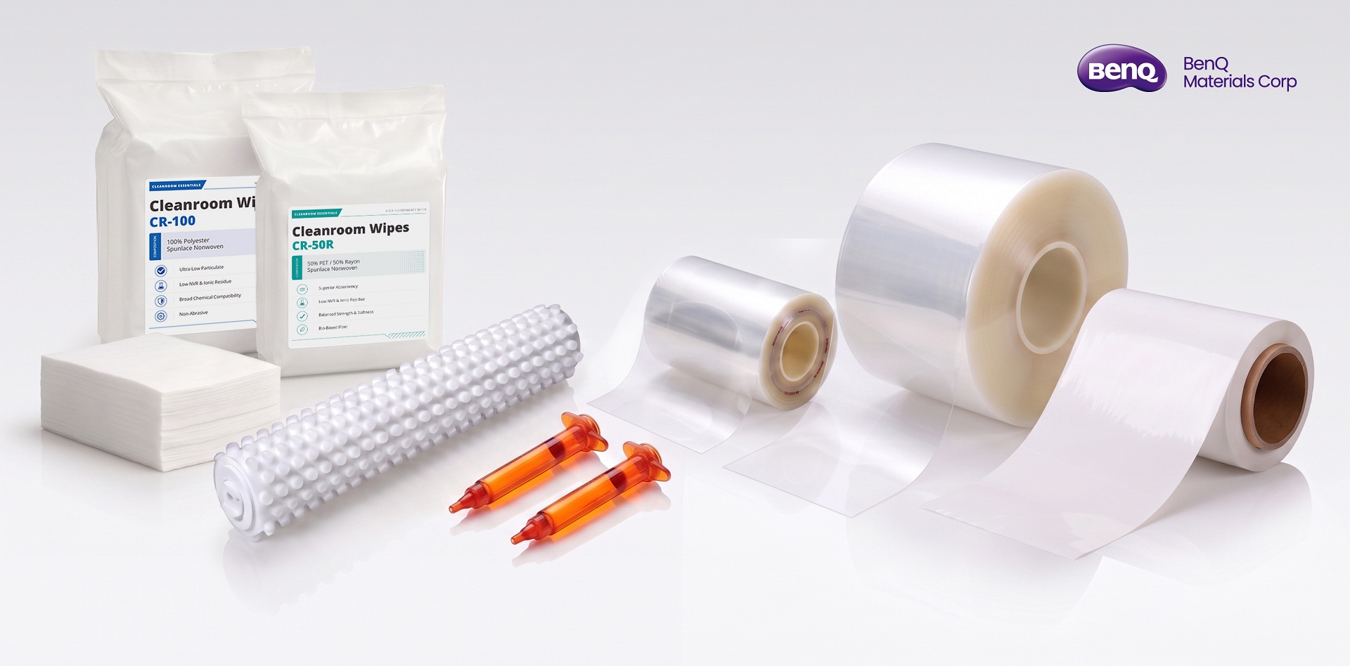
Global material science leader BenQ Materials announced today that it will make its official debut exhibition at SEMICON Taiwan 2026 from September 2 to 4. Centered around the core theme "Precision Materials for Semiconductor Manufacturing," the company will comprehensively showcase critical material solutions for wafer fabrication, advanced packaging, and cleanroom processes. BenQ Materials emphasizes that its core exhibition theme is "Progress Matters"—representing that the company has completed customer validation and production-readiness preparations for multiple products, successfully transforming technological innovations in precision polymer and coating science into tangible manufacturing benefits that help semiconductor customers push process limits and optimize total cost of ownership.
"BenQ Materials has always been committed to pushing the value of material science to its peak," stated ZC Chen, Chairman of BenQ Materials. "We have successfully integrated and expanded our core technologies in medical and optical materials—which demand extreme safety and cleanliness—into the high-precision semiconductor and optical communication packaging markets. Positioned as a strategic partner helping semiconductor customers break through process bottlenecks, BenQ Materials highlights three core pillars this exhibition: 'Increase Yield,' 'Improve Stability,' and 'Reduce Contamination,' aligning our technological advantages directly with the three core objectives of semiconductor manufacturing. Not only can we provide immediate local support, but under the trends of strategic cost control and building high-resilience supply chains, we have also passed customer validation with Tier-1 giants, joining hands to build a semiconductor manufacturing chain characterized by high yields, high stability, and ESG sustainability, and becoming a trusted local high-end material strategic partner for global enterprises."
High-end semiconductor precision materials have long been monopolized by foreign enterprises from Japan and the United States, often adopting a closed-loop model where materials are bundled with specific equipment, placing immense pressure on wafer manufacturers and OSATs during supply chain fluctuations. Ray Liu, GM of BenQ Materials, explained, "With our polymer synthesis and formula fine-tuning production capacity utilizing a '10-ton reactor' in Taiwan, alongside a 100-class cleanroom precision coating end-to-end production line, BenQ Materials' local R&D and technical support teams offer rapid response capabilities. We can provide immediate local support, stable high-purity supply, and highly customized developments tailored specifically to adhesive viscosity, thickness, and expansion characteristics."
Three Core Exhibition Pillars: Product Highlights and Customer Validation Data
Pillar 1: Increase Yield — Safeguarding Extreme Cleanliness in Wafer Processing
Focusing on wafer cleaning processes, this module provides the industry’s highest level of low-particle detection and exceptional cleaning performance.Advanced PVA Brush Roller for CMP Wafer Cleaning: Built upon stringent medical-grade specifications, BenQ Materials has custom-engineered an advanced PVA air-formed brush roller designed specifically for post-CMP (Chemical Mechanical Planarization) cleaning processes in semiconductor fabrication, precisely resolving industry pain points regarding micro-residues and equipment productivity.
- Significantly Shortens Break-in Time and Maximizes Equipment UPH: Addressing the tool utilization metrics most valued by semiconductor fabs, this product utilizes a precision air-formed structure technology (starch-free pore formation) to dramatically shorten the pre-wash break-in period before the brush goes online. In mature processes, break-in time is reduced by 50%; in high-end advanced processes, break-in time is substantially decreased by up to 70% compared to traditional competing products, optimizing UPH and reducing non-productive operational costs.
- Patented Air-Formed and Surface Treatment Technologies for Enhanced Cleaning Efficiency and Green Sustainability: Benefiting from a 100% interconnected pore air-formed patent, the product demonstrates exceptional liquid penetration and fluid transfer characteristics. Under identical water intake conditions, water output is increased by over 50% compared to competing products, while a proprietary surface treatment technology can regulate regional water distribution to ensure chemicals and deionized water accurately cover the wafer surface, boosting cleaning efficacy. Through superior fluid transfer efficiency, daily process water consumption (TIWA) for customers is successfully reduced by approximately 10%, simultaneously maintaining high yields and achieving green sustainability and carbon reduction targets.
- Starch-Free Residue and Anti-Torsion Slippage Design Defending Advanced Process Yields: Produced within an ISO-certified cleanroom, metal ions and micro-particles are strictly controlled to eliminate contamination from the source. The proprietary integrated design of the PVA foam and core creates a sturdier structure, effectively increasing the torsional strength of the brush and entirely eliminating the risk of core-foam separation and idling during processing, providing the highest standard of stable cleaning assurance for advanced nodes.
Cleanroom Wipe: Designed specifically for high-standard cleanroom environment maintenance, utilizing hydroentangled spunlace nonwoven fabric and thermal-pressed bonding treatments to enhance fiber structural stability and reduce fiber shedding and linting during wiping. Its low-particle and low-ion-residue characteristics make it suitable for ISO Class 5–8 cleanroom surrounding environments and workstations, helping to minimize micro-contamination risks during cleaning.
Pillar 2: Improve Stability — Critical Protection for Advanced Packaging and CPO
This module focuses on advanced packaging processes and high-density optical communication packaging, providing ultra-high precision, heat resistance, and residue-free stable adhesive protection.Dicing UV Tape: Designed to provide efficient protection and support during wafer dicing processes. It offers strong adhesion(1100 ± 300 gf/25mm) during high-speed cutting to ensure chips remain firmly secured without splashing or chipping; following rapid UV-cured debonding under specific wavelengths, adhesion drops to an extremely low level(< 15 gf/25mm), supporting high-speed automated pick-up with absolute zero adhesive residue.
BG (Backgrinding) Tape: Targeted at wafer backside thinning and advanced packaging processes, BenQ Materials introduces a high-end grinding protection tape designed to protect precision circuitry and micro-bumps on the wafer front side. This product provides ultimate physical protection and face-support during thinning, preventing high-pressure grinding stress from damaging silicon wafer circuits.
- World-Class Total Thickness Variation (TTV) Control for Uniform Face Support: To prevent stress concentration and wafer breakage caused by uneven tape thickness during physical grinding, BenQ Materials leverages its high-precision coating expertise to precisely control total thickness variation (TTV). High-toughness substrates and a proprietary uniform adhesive layer deliver flat and even face-support, preventing localized wafer deformation.
- Seamless Coverage of 55μm Micro-Bumps without Voids: With a flagship product thickness of 170μm—composed of a 75μm PET substrate, a 95μm proprietary high-molecular acrylic non-UV pressure-sensitive adhesive, and a 38μm release liner—the highly elastic adhesive layer exhibits exceptional flowability, perfectly enveloping micro-bumps up to 55μm in height. Practical validation following 120 hours of aging tests confirms zero void formation around the bumps, preventing grinding coolant infiltration.
- Exceeding Tier-1 Standards with 120°C High-Temperature Resistance and "Zero Residue" Guarantee: Wafer grinding generates intense physical thermal energy; BenQ Materials' BG tape has passed rigorous 30-minute oven simulation tests at 120°C. Under extreme high temperatures and thermal expansion, the adhesive chemical structure remains stable without melting overflow or deformation, achieving 100% surface adhesive-residue-free peeling to prevent secondary contamination of metal ions and particles on the wafer surface.
- Comprehensive Thickness Roadmap through 2027 for Advanced Packaging High Bumps: To match major mainstream packaging tools and diverse wafer processes, BenQ Materials has planned and developed four complete thickness specifications (170μm, 270μm, 440μm, and 595μm), offering flexible customization. Concurrently, advanced packaging high-end grinding protection tape for high bumps exceeding 250μm in height is currently under active development targeting customer verification completion in 2027, comprehensively mapping out next-generation 3D packaging layouts.
UV Adhesive for CPO Packaging Solutions: Designed specifically for fiber array (FAU) and micro-lens array (MLA) coupling and V-groove fixing in next-generation Co-Packaged Optics (CPO) technology. Compared to traditional mainstream Japanese commercial adhesives, this product demonstrates significant performance breakthroughs:
- 5x Ultra-Fast Curing Eliminating Secondary Thermal Curing: Competing products require up to 600 seconds of UV curing and typically demand an additional thermal curing step. BenQ Materials' UCE 1-28 and UCE 2-3 achieve cure times of less than 120 seconds under equivalent 365nm UV lighting power, eliminating secondary thermal baking steps and substantially shortening automated packaging wait times.
- Ultra-Low Volumetric Shrinkage Ensuring Sub-Micron Alignment Precision: Utilizing a proprietary special monomer formulation, volumetric shrinkage is effectively suppressed to prevent micro-displacements of optical components, ensuring sub-micron alignment precision. Compared to market competitors exhibiting roughly 3.0% volumetric shrinkage—which is prone to displacement induced by curing internal stresses—BenQ Materials' product significantly reduces shrinkage, enhancing assembly stability and accuracy.
- Adhesion Strength and Structural Support Far Surpassing Competitors: In terms of adhesion and structural support, BenQ Materials exhibits distinct advantages. Its shear adhesion strength 25°C, reaches over 130 kgf/cm², outperforming rival benchmarks; in storage modulus 25°C performance, both UCE 1-28 and UCE 2-3 far exceed competitor standards, providing superior anti-vibration support. Furthermore, the product maintains a glass transition temperature(Tg)above 200°C and successfully passes reflow soldering heat-resistance tests, complying fully with Telcordia GR-1221 international reliability verification standards.
Pillar 3: Reduce Contamination — The Invisible Defense Line for Wet Process Yields
This module focuses on high-grade chemical and POU (Point-of-Use) filtration, deploying precise pore-size control to block nanoscale impurities.Semiconductor-grade Micro Contamination Control Filter Membrane: Harnessing its exclusively mastered core technologies of roll-to-roll processing, polymer structure control, and extrusion stretching, BenQ Materials introduces a semiconductor-grade polyolefin porous filter membrane.
- Dual Balance of High Throughput and High Retention: Successfully overcoming industry bottlenecks, it achieves high throughput while stably maintaining near 100% high-efficiency nanoscale particle retention over extended periods, effectively resolving performance roadblocks in semiconductor micro-contamination control.
- 2nm Advanced Process Defense Line: Tailored specifically for advanced node bulk chemical filtration and the final POU filtration stage (precisely trapping nanoscale particles) prior to chemical agents (such as photoresists) entering the wafer.
- Low Carbon and High Chemical Stability: Utilizing polyolefin low-carbon materials with exceptional cleanliness, exhibiting superior corrosion resistance and anti-solvent leach-out properties.
BenQ Materials firmly believes that excellence in material science must withstand production-line verification, and we cordially invite partners across the global semiconductor, advanced packaging, and optoelectronics industries to visit our booth and witness how material science defines the infinite possibilities of the future.
- Exhibition Name: SEMICON Taiwan 2026
- Dates: September 2-4, 2026
- Media Tour Time: September 2, 2026, 1300-1330
- Booth Location:Hall 1, 1F, Taipei Nangang Exhibition Center (TaiNEX Hall 1) [Booth No. M0657]
- Official Website:www.benqmaterials.com
