





Category
Semicon 2026
2026.08.13
Semicon 2026
BG Tape
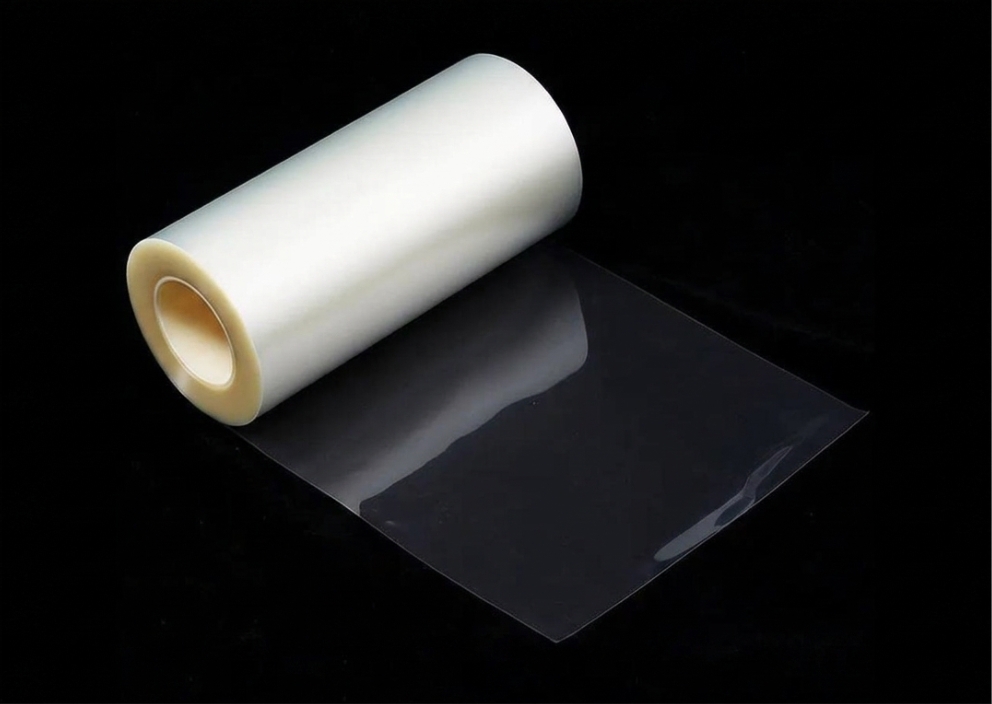
BG Tape
Reliable wafer support and surface protection prevent peeling and damage during back grinding, while excellent bump coverage helps eliminate void formation. Clean release with no adhesive residue supports reliable advanced packaging processes.
Key Features
-
Superior Bump Gap Filling Ability
Specially engineered with a Stress-Absorbing Layer that seamlessly wraps around high bumps, micro-bumps, and high-topography circuitry. This provides complete coverage, effectively preventing slurry penetration during grinding and mitigating the risk of wafer breakage. -
Zero Residue
Formulated with a proprietary polymer adhesive system that leaves zero residue on the wafer surface upon debonding, fully protecting sensitive circuit structures. -
Ultra-Low Total Thickness Variation (TTV)
Engineered with ultra-tight thickness tolerances across both substrate and adhesive layers. This guarantees exceptional post-grind wafer flatness and consistency, perfectly meeting the stringent demands of ultra-thin wafer processing.
Applications & Scenarios 1
-
Ultra-Thin Wafer Thinning for Advanced Packagingotection
-
High Bump & Wafer-Level Packaging (WLP) Circuit Pr
